A Brief Analysis of Power Amplifiers in RF Chips
In the wireless devices we use, we often come across a term - what is the power of the device in watts? And we often think that the greater the power of the device, the better. But is this really the case? Today, we will introduce to you the knowledge about power amplifiers.
I. What is an RF Power Amplifier
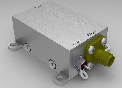
A power amplifier is an amplifier that amplifies the input signal and provides sufficient power to the load. The radio frequency power amplifier (RF PA) is a crucial component in the transmitting system, and its importance is self-evident. In the pre-amplifier circuit of the transmitter, the radio frequency signal power generated by the modulation oscillation circuit is very small. It needs to undergo a series of amplifications (buffer stage, intermediate amplification stage, final power amplification stage) to obtain sufficient radio frequency power before being fed to the antenna for radiation. To obtain a sufficiently large radio frequency output power, a radio frequency power amplifier must be used. After the modulator generates the radio frequency signal, the radio frequency modulated signal is amplified to a sufficient power by the RF PA, and then it passes through the matching network before being transmitted by the antenna.

The function of an amplifier is to amplify the input content and output it. The input and output contents are referred to as "signals", often represented as voltage or power. The main technical indicators of a radio frequency power amplifier are output power and efficiency. How to increase the output power and efficiency is the core of the design goal for radio frequency power amplifiers. Usually, in radio frequency power amplifiers, an LC resonant circuit can be used to select the fundamental frequency or a certain harmonic to achieve distortion-free amplification. In addition, the harmonic components in the output should also be as small as possible to avoid interference to other channels.
Depending on the working conditions, power amplifiers can be classified into: linear power amplifiers and switch-mode power amplifiers.
The linear power amplifier operates at a high frequency but has a relatively narrow bandwidth. RF power amplifiers typically use frequency-selective networks as the load circuit. Linear RF power amplifiers can be classified into three working states based on the different current conduction angles: Class A (A), Class B (B), and Class C (C). Class A amplifier has a current conduction angle of 360°, which is suitable for small-signal low-power amplification. Class B amplifier has a current conduction angle of 180°, while Class C amplifier has a current conduction angle less than 180°. Both Class B and Class C are suitable for high-power operation, and the output power and efficiency of Class C operation are the highest among the three states. Most RF power amplifiers operate in Class C, but the current waveform distortion of Class C amplifiers is too large, and they can only be used for power amplification with a tuned circuit as the load resonant circuit. Since the tuned circuit has filtering capabilities, the loop current and voltage are still close to a sine wave, and the distortion is very small.
Switching Mode Power Amplifier (SMPA) operates electronic devices in a switching state. Common types include D-class and E-class amplifiers. The efficiency of D-class amplifiers is higher than that of C-class amplifiers. SMPA drives active transistors in a switching mode, with the transistors operating in either an on or off state. The voltage and current time-domain waveforms do not overlap, so the DC power consumption is zero, and the ideal efficiency can reach 100%.
Overall, traditional linear power amplifiers have high gain and linearity but low efficiency, while switch-mode power amplifiers have high efficiency and high output power, but poor linearity.
II. Process of Power Amplifier
At present, the mainstream process for power amplifiers is still GaAs process. Additionally, GaAs HBT, or Gallium Arsenide Heterojunction Bipolar Transistor. HBT is a bipolar transistor composed of a GaAs layer and an AlGaAs layer. Although CMOS process is relatively mature, the application of Si CMOS power amplifiers is not widespread. In terms of cost, although the silicon wafers used in CMOS process are relatively cheaper, the layout area of CMOS power amplifiers is relatively large. Moreover, the complex design of CMOS PA requires high R&D costs, making the overall cost advantage of CMOS power amplifiers not so obvious. In terms of performance, CMOS power amplifiers have poorer performance in terms of linearity, output power, and efficiency. Additionally, CMOS process has inherent disadvantages such as a higher knee point voltage, a lower breakdown voltage, and a lower resistivity of the substrate of the CMOS process.

III. Development Trends of Power Amplifiers
The British research company Technavio states that the global power amplifier market has three main trends: the increase in wafer size; the adoption of CMOS technology by start-ups; and the growing demand for high-speed amplifiers in the defense sector: using the InGaP process to achieve low power consumption and high efficiency in power amplifiers.
The size of wafers has increased. The semiconductor industry has witnessed the changes in wafer size over the past 40 years. The size of gallium arsenide (GaAs) wafers has expanded from 50mm to 150mm, and the manufacturing cost has decreased by 20% to 25%. Currently, the industry typically uses 150mm wafers for the manufacture of power amplifiers. It is predicted that 150mm wafers will continue to be used, as manufacturers such as Taiwan's Sunway Semiconductor are investing heavily in upgrading and building 150mm factories. The industry is developing 200mm wafer technology, and it is expected to be able to conduct trial production by the end of 2018. Researchers at Stanford University are studying ways to reduce the price of 200mm GaAs wafers, enabling them to compete in the market with silicon wafers at a lower price. This also raises the demand for mask inspection equipment and wafer manufacturing equipment.
Start-up companies adopt CMOS technology. Some start-ups, such as Acco Semiconductor, are increasingly adopting CMOS technology. Acco Semiconductor seized the opportunity presented by the huge demand for RF power amplifiers in mobile phones and IoT products and has invested 35 billion US dollars to expand its CMOS-based RF power amplifier business. Currently, the vast majority of power amplifiers use silicon germanium (SiGe) or GaAs technology instead of CMOS. However, according to reports, CMOS-based processes can help achieve low-cost and high-performance power amplifiers.
The defense sector requires high-speed amplifiers. The military sector needs to make more efficient use of the spectrum and utilize more mobile devices for communication. Therefore, Technavio states that the military sector demands high-speed power amplifiers. The US Defense Advanced Research Projects Agency (DARPA) has made progress in the terahertz electronics project, where the US Northrop Grumman Corporation has developed solid-state power amplifiers and traveling wave tube amplifiers, which are the only two terahertz frequency products. Terahertz frequency amplifiers can be used in many fields, including high-resolution security imaging, high-data-rate communication, collision avoidance radar, long-distance detection systems for hazardous chemicals and explosives, etc. The high-speed operation of these devices requires the use of high-speed amplifiers.
By utilizing the InGaP process, low power consumption and high efficiency of power amplifiers can be achieved. InGaP is particularly suitable for high-frequency applications that require considerable power output. The improvement of the InGaP process has led to an increase in production and a higher degree of integration, enabling the chips to integrate more functions. This simplifies system design, reduces raw material costs, and saves board space. Some InGaP PA also adopt multi-chip packages that include CMOS control circuits. Nowadays, front-end WLAN modules that integrate PA and low-noise amplifier (LNA) and combine RF switches at the receiving end can adopt compact packaging. For example, the InGaP-Plus process proposed by ANADIGICS can integrate bipolar transistors and field-effect transistors on the same InGaP chip. This technology is being used in new CDMA and WCDMA power amplifiers with improved size and PAE (Power Amplifier Efficiency).
IV. Main Specifications of the Power Amplifier
Operating frequency range. Generally speaking, it refers to the linear operating frequency range of the amplifier. If the frequency starts from DC, then the amplifier is considered a DC amplifier.
Gain. The operating gain is the primary metric for measuring the amplification capability of an amplifier. Gain is defined as the ratio of the power transmitted from the amplifier's output port to the load to the actual power transmitted from the signal source to the amplifier's input port. Gain flatness refers to the range of changes in the amplifier's gain over the entire operating frequency band at a certain temperature, and it is also a key indicator of the amplifier.
Output power and 1dB compression point (P1dB). When the input power exceeds a certain level, the gain of the transistor begins to decline, and eventually the output power reaches saturation. When the gain of the amplifier deviates from a constant value or is 1dB lower than other small signal gains, this point is the well-known 1dB compression point (P1dB).
Efficiency. Since the power amplifier is a power component, it requires the consumption of power supply current. Therefore, the efficiency of the power amplifier is extremely important for the overall efficiency of the system. Power efficiency is the ratio of the RF output power of the power amplifier to the DC power supplied to the transistors.
Intermodulation distortion. Intermodulation distortion refers to the mixed components generated when two or more input signals of different frequencies pass through a power amplifier. This is caused by the non-linear characteristics of the power amplifier.
The third-order intermodulation cutoff point (IP3). IP3 is also an important indicator of the nonlinearity of power amplifiers. When the output power is constant, the larger the output power at the third-order intermodulation cutoff point, the better the linearity of the power amplifier.
Dynamic range. The dynamic range of a power amplifier generally refers to the difference between the minimum detectable signal and the maximum input power within the linear operating range. Naturally, this value should be as large as possible.
Harmonic distortion. When the input signal increases to a certain level, the power amplifier will generate a series of harmonics due to operating in the nonlinear region. For large power amplifier systems, generally, filters are needed to reduce the harmonics to below 60 dBc.
Input/output standing wave ratio. Indicates the matching degree between the power amplifier and the entire system. A deteriorated input/output ratio will cause fluctuations in the system's gain and degradation in group delay. However, designing a high standing wave ratio power amplifier is quite challenging. In most systems, it is generally required that the input standing wave ratio of the power amplifier be lower than 2:1.
-
 2025-10-24
 -

What is an Emergency Communication System and How Does It Work?
2025-09-16 -

What Is Point to Point and Point to Multipoint Wireless Network?
2025-09-05 -

What Are the Two Types of Microwave Transmission?
2025-08-29 -

Multi-Node MESH Networking: Principles and Real-World Applications
2025-08-18 -

What Is the Difference Between Radio and Microwave Video Transmission?
2025-07-30 -

Unmanned Aerial Vehicle Transmission Equipment Communication Solution
2025-07-24


